Saturday 3 November 2012

2.2 X-Y PLOTS AND ANNOTATIONS

2.2 X-Y PLOTS AND ANNOTATIONS


The plot command generates a linear x-y plot. There are three variations of the
plot command.
(a) plot(x)
(b) plot(x, y)
(c) plot(x1, y1, x2, y2, x3, y3, ..., xn, yn)
If x is a vector, the command
plot(x)
will produce a linear plot of the elements in the vector x as a function of the
index of the elements in x. MATLAB will connect the points by straight lines.
If x is a matrix, each column will be plotted as a separate curve on the same
graph. For example, if
x = [ 0 3.7 6.1 6.4 5.8 3.9 ];
then, plot(x) results in the graph shown in Figure 2.1.
If x and y are vectors of the same length, then the command
plot(x, y)
plots the elements of x (x-axis) versus the elements of y (y-axis). For example,
the MATLAB commands
t = 0:0.5:4;
y = 6*exp(-2*t);
plot(t,y)
will plot the function y(t) = 6e−2t at the following times: 0, 0.5, 1.0, …, 4 .
The plot is shown in Figure 2.2.
To plot multiple curves on a single graph, one can use the plot command
with multiple arguments, such as
plot(x1, y1, x2, y2, x3, y3, ..., xn, yn)
The variables x1, y1, x2, y2, etc., are pairs of vector. Each x-y pair is
graphed, generating multiple lines on the plot. The above plot command
allows vectors of different lengths to be displayed on the same graph.
MATLAB automatically scales the plots. Also, the plot remains as the current
plot until another plot is generated; in which case, the old plot is erased. The
hold command holds the current plot on the screen, and inhibits erasure and
rescaling. Subsequent plot commands will overplot on the original curves.
The hold command remains in effect until the command is issued again.
When a graph is drawn, one can add a grid, a title, a label and x- and y-axes
to the graph. The commands for grid, title, x-axis label, and y-axis label are
grid (grid lines), title (graph title), xlabel (x-axis label), and ylabel (y-axis
label), respectively. For example, Figure 2.2 can be titled, and axes labeled
with the following commands:
t = 0:0.5:4;
y = 6*exp(-2*t);
plot(t, y)
title('Response of an RC circuit')
xlabel('time in seconds')
ylabel('voltage in volts')
grid

To write text on a graphic screen beginning at a point (x, y) on the graphic
screen, one can use the command
text(x, y, ’text’)
For example, the statement
text(2.0, 1.5, ’transient analysis’)
will write the text, transient analysis, beginning at point (2.0,1.5). Multiple
text commands can be used. For example, the statements
plot(a1,b1,a2,b2)
text(x1,y1,’voltage’)
text(x2,y2,’power’)

will provide texts for two curves: a1 versus b1 and a2 versus b2. The text will
be at different locations on the screen provided x1 ≠ x2 or y1 ≠ y2.
If the default line-types used for graphing are not satisfactory, various symbols
may be selected. For example:
plot(a1, b1, ’*’)
draws a curve, a1 versus b1, using star(*) symbols, while
plot(a1, b1, ’*’, a2, b2, ’+’)
uses a star(*) for the first curve and the plus(+) symbol for the second curve.
Other print types are shown in Table 2.2.

CHAPTER TWO- PLOTTING COMMANDS

2.1 GRAPH FUNCTIONS


MATLAB has built-in functions that allow one to generate bar charts, x-y,
polar, contour and 3-D plots, and bar charts. MATLAB also allows one to
give titles to graphs, label the x- and y-axes, and add a grid to graphs. In
addition, there are commands for controlling the screen and scaling. Table 2.1
shows a list of MATLAB built-in graph functions. One can use MATLAB’s
help facility to get more information on the graph functions.

Table 2.1
Plotting Functions
FUNCTION
DESRIPTION
axis- freezes the axis limits
bar -plots bar chart
contour- performs contour plots
ginput- puts cross-hair input from mouse
grid- adds grid to a plot
gtext -does mouse positioned text
histogram -gives histogram bar graph
hold- holds plot (for overlaying other plots)
loglog- does log versus log plot
mesh- performs 3-D mesh plot
meshdom- domain for 3-D mesh plot
pause- wait between plots
plot- performs linear x-y plot
polar -performs polar plot
semilogx- does semilog x-y plot (x-axis logarithmic)
semilogy- does semilog x-y plot (y-axis logarithmic)
shg -shows graph screen
stairs- performs stair-step graph
text- positions text at a specified location on graph
title -used to put title on graph
xlabel- labels x-axis
ylabel -labels y-axis

1.6.2 Function Files

1.6.2 Function Files


Function files are m-files that are used to create new MATLAB functions.
Variables defined and manipulated inside a function file are local to the function,
and they do not operate globally on the workspace. However, arguments
may be passed into and out of a function file.
The general form of a function file isfunction variable(s) = function_name (arguments)
% help text in the usage of the function
%
.
.
end
To illustrate the usage of function files and rules for writing m-file function, let
us study the following two examples.
Example 1.3
Write a function file to solve the equivalent resistance of series connected resistors,
R1, R2, R3, …, Rn.
Solution:
MATLAB Script
function req = equiv_sr(r)
% equiv_sr is a function program for obtaining
% the equivalent resistance of series
% connected resistors
% usage: req = equiv_sr(r)
% r is an input vector of length n
% req is an output, the equivalent resistance(scalar)
%
n = length(r); % number of resistors
req = sum (r); % sum up all resistors
end
The above MATLAB script can be found in the function file equiv_sr.m,
which is available on the disk that accompanies this book.
Suppose we want to find the equivalent resistance of the series connected resistors
10, 20, 15, 16 and 5 ohms. The following statements can be typed in the
MATLAB command window to reference the function equiv_sr
a = [10 20 15 16 5];
Rseries = equiv_sr(a)
diary
The result obtained from MATLAB is
© 1999
Rseries =
66
Example 1.4
Write a MATLAB function to obtain the roots of the quadratic equation
ax2 + bx + c = 0
Solution:
MATLAB Script
function rt = rt_quad(coef)
%
% rt_quad is a function for obtaining the roots of
% of a quadratic equation
% usage: rt = rt_quad(coef)
% coef is the coefficients a,b,c of the quadratic
% equation ax*x + bx + c =0
% rt are the roots, vector of length 2
% coefficient a, b, c are obtained from vector coef
a = coef(1); b = coef(2); c = coef(3);
int = b^2 - 4*a*c;
if int > 0
srint = sqrt(int);
x1= (-b + srint)/(2*a);
x2= (-b - srint)/(2*a);
elseif int == 0
x1= -b/(2*a);
x2= x1;
elseif int < 0
srint = sqrt(-int);
p1 = -b/(2*a);
p2 = srint/(2*a);
x1 = p1+p2*j;
x2 = p1-p2*j;
end
rt =[x1;
x2];
end

1.6 M-FILES


Normally, when single line commands are entered, MATLAB processes the
commands immediately and displays the results. MATLAB is also capable of
processing a sequence of commands that are stored in files with extension m.
MATLAB files with extension m are called m-files. The latter are ASCII text
files, and they are created with a text editor or word processor. To list m-files
in the current directory on your disk, you can use the MATLAB command
what. The MATLAB command, type, can be used to show the contents of a
specified file. M-files can either be script files or function files. Both script
and function files contain a sequence of commands. However, function files
take arguments and return values.

1.6.1 Script files
Script files are especially useful for analysis and design problems that require
long sequences of MATLAB commands. With script file written using a text
editor or word processor, the file can be invoked by entering the name of the
m-file, without the extension. Statements in a script file operate globally on
the workspace data. Normally, when m-files are executing, the commands are
not displayed on screen. The MATLAB echo command can be used to view
m-files while they are executing. To illustrate the use of script file, a script
file will be written to simplify the following complex valued expression z.
Example 1.2
Simplify the complex number z and express it both in rectangular and polar
form.
z
j j
j j
=
+ + ∠
+ +
( )( )( )
( )( )
3 4 5 2 2 60
3 6 1 2
0
Solution:
The following program shows the script file that was used to evaluate the
complex number, z, and express the result in polar notation and rectangular
form.
MATLAB Script
diary ex1_2.dat


% Evaluation of Z
% the complex numbers are entered
Z1 = 3+4*j;
Z2 = 5+2*j;
theta = (60/180)*pi; % angle in radians
Z3 = 2*exp(j*theta);
Z4 = 3+6*j;
Z5 = 1+2*j;
% Z_rect is complex number Z in rectangular form
disp('Z in rectangular form is'); % displays text inside brackets
Z_rect = Z1*Z2*Z3/(Z4+Z5);
Z_rect
Z_mag = abs (Z_rect); % magnitude of Z
Z_angle = angle(Z_rect)*(180/pi); % Angle in degrees
disp('complex number Z in polar form, mag, phase'); % displays text
%inside brackets
Z_polar = [Z_mag, Z_angle]
diary
The program is named ex1_2.m. It is included in the disk that accompanies
this book. Execute it by typing ex1_2 in the MATLAB command window.
Observe the result, which should be
Z in rectangular form is
Z_rect =
1.9108 + 5.7095i
complex number Z in polar form (magnitude and phase) is
Z_polar =
6.0208 71.4966


1.5 THE COLON SYMBOL (:)

1.5 THE COLON SYMBOL (:)

The colon symbol (:) is one of the most important operators in MATLAB. It
can be used (1) to create vectors and matrices, (2) to specify sub-matrices and
vectors, and (3) to perform iterations. The statement
t1 = 1:6
will generate a row vector containing the numbers from 1 to 6 with unit increment.
MATLAB produces the result
t1 =
1 2 3 4 5 6
Non-unity, positive or negative increments, may be specified. For example,
the statement
t2 = 3:-0.5:1
will result in
t2 =
3.0000 2.5000 2.0000 1.5000 1.0000
The statement
t3 = [(0:2:10);(5:-0.2:4)]
will result in a 2-by-4 matrix
t3 =
0 2.0000 4.0000 6.0000 8.0000 10.0000
5.0000 4.8000 4.6000 4.4000 4.2000 4.0000
Other MATLAB functions for generating vectors are linspace and logspace.
Linspace generates linearly evenly spaced vectors, while logspace generates
logarithmically evenly spaced vectors. The usage of these functions is of the
form:
linspace(i_value, f_value, np)
logspace(i_value, f_value, np)
where
i_value is the initial value
f_value is the final value
np is the total number of elements in the vector.
For example,
t4 = linspace(2, 6, 8)
will generate the vector
t4 =
Columns 1 through 7
2.0000 2.5714 3.1429 3.7143 4.2857 4.8571
5.4286
Column 8
6.0000
Individual elements in a matrix can be referenced with subscripts inside parentheses.
For example, t2(4) is the fourth element of vector t2. Also, for matrix
t3, t3(2,3) denotes the entry in the second row and third column. Using the colon
as one of the subscripts denotes all of the corresponding row or column.
For example, t3(:,4) is the fourth column of matrix t3. Thus, the statement
t5 = t3(:,4)
will give
t5 =
6.0000
4.4000
Also, the statement t3(2,:) is the second row of matrix t3. That is the statement
t6 = t3(2,:)
will result in
t6 =
5.0000 4.8000 4.6000 4.4000 4.2000 4.0000
If the colon exists as the only subscript, such as t3(:), the latter denotes the
elements of matrix t3 strung out in a long column vector. Thus, the statement
t7 = t3(:)
will result in
t7 =
0
5.0000
2.0000
4.8000
4.0000
4.6000
6.0000
4.4000
8.0000
4.2000
10.0000
4.0000
Example 1.1
The voltage, v, across a resistance is given as (Ohm’s Law), v = Ri , where
i is the current and R the resistance. The power dissipated in resistor R is
given by the expression
P = Ri2
If R = 10 Ohms and the current is increased from 0 to 10 A with increments
of 2A, write a MATLAB program to generate a table of current, voltage and
power dissipation.
Solution:
MATLAB Script
diary ex1_1.dat
% diary causes output to be written into file ex1_1.dat
% Voltage and power calculation
R=10; % Resistance value
i=(0:2:10); % Generate current values
v=i.*R; % array multiplication to obtain voltage
p=(i.^2)*R; % power calculation
sol=[i v p] % current, voltage and power values are printed
diary
% the last diary command turns off the diary state
MATLAB produces the following result:
sol =
Columns 1 through 6
0 2 4 6 8 10
Columns 7 through 12
0 20 40 60 80 100
Columns 13 through 18
0 40 160 360 640 1000
Columns 1 through 6 constitute the current values, columns 7 through 12 are
the voltages, and columns 13 through 18 are the power dissipation values

1.4 COMPLEX NUMBERS

1.4 COMPLEX NUMBERS

MATLAB allows operations involving complex numbers. Complex numbers
are entered using function i or j. For example, a number z = 2 + j2 may be
entered in MATLAB as
z = 2+2*i
or
z = 2+2*j
Also, a complex number za
za = 2 2 exp[(π / 4) j]
can be entered in MATLAB as
za = 2*sqrt(2)*exp((pi/4)*j)
It should be noted that when complex numbers are entered as matrix elements
within brackets, one should avoid any blank spaces. For example,
y = 3 + j4 is represented in MATLAB as
y = 3+4*j
If spaces exist around the + sign, such as
u= 3 + 4*j
MATLAB considers it as two separate numbers, and y will not be equal to u.
If w is a complex matrix given as
w =
1 1 2 2
3 2 4 3
+ −
+ +
 
 
j j
j j
then we can represent it in MATLAB as
w = [1+j 2-2*j; 3+2*j 4+3*j]
which will produce the result
w =
1.0000 + 1.0000i 2.0000 - 2.0000i
3.0000 + 2.0000i 4.0000 + 3.0000i
If the entries in a matrix are complex, then the “prime” (‘) operator produces
the conjugate transpose. Thus,
wp = w'
will produce
wp =
1.0000 - 1.0000i 3.0000 - 2.0000i
2.0000 + 2.0000i 4.0000 - 3.0000i
For the unconjugate transpose of a complex matrix, we can use the point transpose
(.’) command. For example,
wt = w.'
will yield
© 1999
wt =
1.0000 + 1.0000i 3.0000 + 2.0000i
2.0000 - 2.0000i 4.0000 + 3.0000i

1.3 ARRAY OPERATIONS

1.3 ARRAY OPERATIONS


Array operations refer to element-by-element arithmetic operations. Preceding
the linear algebraic matrix operations, * / \ ‘ , by a period (.) indicates an array
or element-by-element operation. Thus, the operators .* , .\ , ./, .^ , represent
element-by-element multiplication, left division, right division, and raising to
the power, respectively. For addition and subtraction, the array and matrix operations
are the same. Thus, + and .+ can be regarded as an array or matrix
addition.
If A1 and B1 are matrices of the same dimensions, then A1.*B1 denotes an array
whose elements are products of the corresponding elements of A1 and B1.
Thus, if
A1 = [2 7 6
8 9 10];
B1 = [6 4 3
2 3 4];
then
C1 = A1.*B1
results in
C1 =
12 28 18
16 27 40
An array operation for left and right division also involves element-by-element
operation. The expressions A1./B1 and A1.\B1 give the quotient of elementby-
element division of matrices A1 and B1. The statementD1 = A1./B1
gives the result
D1 =
0.3333 1.7500 2.0000
4.0000 3.0000 2.5000
and the statement
E1 = A1.\B1
gives
E1 =
3.0000 0.5714 0.5000
0.2500 0.3333 0.4000
The array operation of raising to the power is denoted by .^. The general
statement will be of the form:
q = r1.^s1
If r1 and s1 are matrices of the same dimensions, then the result q is also a matrix
of the same dimensions. For example, if
r1 = [ 7 3 5];
s1 = [ 2 4 3];
then
q1 = r1.^s1
gives the result
q1 =
49 81 125
© 1999
One of the operands can be scalar. For example,
q2 = r1.^2
q3 = (2).^s1
will give
q2 =
49 9 25
and
q3 =
4 16 8
Note that when one of the operands is scalar, the resulting matrix will have the
same dimensions as the matrix operand.

1.2 MATRIX OPERATIONS
The basic matrix operations are addition(+), subtraction(-), multiplication (*),
and conjugate transpose(‘) of matrices. In addition to the above basic operations,
MATLAB has two forms of matrix division: the left inverse operator \
or the right inverse operator /.
Matrices of the same dimension may be subtracted or added. Thus if E and F
are entered in MATLAB as
E = [7 2 3; 4 3 6; 8 1 5];
F = [1 4 2; 6 7 5; 1 9 1];
and
G = E - F
H = E + F
then, matrices G and H will appear on the screen as
G =
6 -2 1
-2 -4 1
7 -8 4
H =
8 6 5
10 10 11
9 10 6
A scalar (1-by-1 matrix) may be added to or subtracted from a matrix. In this
particular case, the scalar is added to or subtracted from all the elements of another
matrix. For example,
J = H + 1
gives
J =
9 7 6
11 11 12
10 11 7
Matrix multiplication is defined provided the inner dimensions of the two operands
are the same. Thus, if X is an n-by-m matrix and Y is i-by-j matrix


X*Y is defined provided m is equal to i. Since E and F are 3-by-3 matrices,
the product
Q = E*F
results as
Q =
22 69 27
28 91 29
19 84 26
Any matrix can be multiplied by a scalar. For example,
2*Q
gives
ans =
44 138 54
56 182 58
38 168 52
Note that if a variable name and the “=” sign are omitted, a variable name ans
is automatically created.
Matrix division can either be the left division operator \ or the right division
operator /. The right division a/b, for instance, is algebraically equivalent to
a
b
while the left division a\b is algebraically equivalent to
b
a
.
If Z * I = V and Z is non-singular, the left division, Z\V is equivalent to
MATLAB expression
I = inv(Z) *V
where inv is the MATLAB function for obtaining the inverse of a matrix. The
right division denoted by V/Z is equivalent to the MATLAB expression
I = V *inv(Z)
There are MATLAB functions that can be used to produce special matrices.
Examples are given in Table 1.3.


1.1 MATLAB BASIC OPERATIONS


When MATLAB is invoked, the command window will display the prompt >>.
MATLAB is then ready for entering data or executing commands. To quit
MATLAB, type the command

exit or quit

MATLAB has on-line help. To see the list of MATLAB’s help facility, type

help


The help command followed by a function name is used to obtain information
on a specific MATLAB function. For example, to obtain information on
the use of fast Fourier transform function, fft, one can type the command

help fft


The basic data object in MATLAB is a rectangular numerical matrix with real
or complex elements. Scalars are thought of as a 1-by-1 matrix. Vectors are
considered as matrices with a row or column. MATLAB has no dimension
statement or type declarations. Storage of data and variables is allocated
automatically once the data and variables are used.

MATLAB statements are normally of the form:

variable = expression


Expressions typed by the user are interpreted and immediately evaluated by the
MATLAB system. If a MATLAB statement ends with a semicolon, MATLAB
evaluates the statement but suppresses the display of the results. MATLAB
is also capable of executing a number of commands that are stored in a file.
This will be discussed in Section 1.6. A matrix


A =
1 2 3
2 3 4
3 4 5






may be entered as follows:


A = [1 2 3; 2 3 4; 3 4 5];
Note that the matrix entries must be surrounded by brackets [ ] with row
elements separated by blanks or by commas. The end of each row, with the
exception of the last row, is indicated by a semicolon. A matrix A can also be
entered across three input lines as


A = [ 1 2 3
2 3 4
3 4 5];

In this case, the carriage returns replace the semicolons. A row vector B with
four elements

B = [ 6 9 12 15 18}
can be entered in MATLAB as
B = [6 9 12 15 18];
or

B = [6 , 9,12,15,18]
For readability, it is better to use spaces rather than commas between the elements.
The row vector B can be turned into a column vector by transposition,
which is obtained by typing
C = B’


The above results in
C =
6
9
12
15
18


Other ways of entering the column vector C are
C = [6
9
12
15
18]


or
C = [6; 9; 12; 15; 18]


MATLAB is case sensitive in naming variables, commands and functions.
Thus b and B are not the same variable. If you do not want MATLAB to be
case sensitive, you can use the command

casesen off


To obtain the size of a specific variable, type size ( ). For example, to find the
size of matrix A, you can execute the following command:

size(A)

The result will be a row vector with two entries. The first is the number of
rows in A, the second the number of columns in A.
To find the list of variables that have been used in a MATLAB session, type
the command
whos
There will be a display of variable names and dimensions. Table 1.1 shows
the display of the variables that have been used so far in this book:


MATLAB FUNDAMENTALS

MATLAB FUNDAMENTALS

MATLAB is a numeric computation software for engineering and scientific
calculations. The name MATLAB stands for MATRIX LABORATORY.
MATLAB is primarily a tool for matrix computations. It was developed by
John Little and Cleve Moler of MathWorks, Inc. MATLAB was originally
written to provide easy access to the matrix computation software packages
LINPACK and EISPACK.

MATLAB is a high-level language whose basic data type is a matrix that does
not require dimensioning. There is no compilation and linking as is done in
high-level languages, such as C or FORTRAN. Computer solutions in
MATLAB seem to be much quicker than those of a high-level language such
as C or FORTRAN. All computations are performed in complex-valued double
precision arithmetic to guarantee high accuracy.

MATLAB has a rich set of plotting capabilities. The graphics are integrated in
MATLAB. Since MATLAB is also a programming environment, a user can
extend the functional capabilities of MATLAB by writing new modules.
MATLAB has a large collection of toolboxes in a variety of domains. Some
examples of MATLAB toolboxes are control system, signal processing, neural
network, image processing, and system identification. The toolboxes consist
of functions that can be used to perform computations in a specific domain.

Saturday 27 October 2012

Chapter 6

Chapter 6

Determination of Interface Trapped Charges in
Ultrathin Oxide MOSFETs

Traps at the SiSiO2 interface play an important role in determining the threshold voltage, inversionlayer mobility and lowfrequency
noise of MOSFETs. Proper device modeling requires the knowledge of the density of interface states throughout the bandgap.

In MOSFETs, interface traps have been characterized in three ways:

1) As an average value over both the surface energy bandgap and channel length, Nit (cm 2 ) [23, 5]
2) As an average over the bandgap, but not channel length, Nit(x) (cm 2 ) [5]
3) As an average over channel length, but not surface potential energy in the bandgap, Dit(y) (eV 1 cm 2 ) [24, 25 and 26]


Usually two methods are widely in use as deterministic tools for interface trapped charges. These are:

1) Charge Pumping or CP Method
2) CapacitanceVoltage or CV Method


To mention that in place of using CVmethod, we have employed an improved version of lowfrequency CV method.

This chapter deals with different experiments run on different ultrathin oxide MOSFETs with the above processes.


5.7.1 Gate Current, IG

5.7.1 Gate Current, IG

Based on the lucky electron model, electrons acquire enough energy from the electric field in the channel to surmount the SiSiO2 barrier. Once the required energy to surmount the barrier has been obtained the electrons are redirected towards the SiSiO2 interface by some from of phonon scattering [17, 21].

These electrons, which surmount the SiSiO2 barrier, are injected into the oxide causing gate current, IG [21].

5.8 Fixed Oxide charge (Qf, Nf)

Fixed Charge is a positive charge in the oxide layer less than 2nm from the SiSiO2 interface. This charge is not in electrical communication with underlying charge. It is also assumed to be unchanged by gate bias [22]. Typically, a value of 1.82x10 10 eV 1 cm 2 is representative for the interface charge found in ultrathin oxide silicon MOS devices.

5.7 Relationship between Gate Leakage Current and Interface States

5.7 Relationship between Gate Leakage Current and Interface States

Gate leakage current had not been a major concern in the past as the amount is small and
insignificant. However, it increases in integration density of the Integrated Circuits and reduction of size of the MOSFETs makes leakage current associated to the interface states to be significant [21].

Reduction in transistor size entails very important electric field in the transistor channel. This caused injection of hot carriers in the gate oxide and creates defects in the SiSiO2 interface (interface states). The defects I the SiSiO2 interface in turn cause leakage current in the gate [19, 21].


This gate current is responsible for the degradation in device operating characteristics with time. This “reliability” issue is of considerably importance as the lifetime of electronic parts has to be guaranteed [19, 21].

5.6.2 Depletion

5.6.2 Depletion

When the gate voltage, VG, is slightly more than zero, this causes a net negative charge at the surface of the semiconductor due to the depletion of holes from the region near the surface leaving behind uncompensated ionized acceptors [8]. The MOSFET is said to operate in the depletion mode.

Donor type interface states will be below EFS and will be filled with electrons and be neutral. Acceptor type interface states will be above EFS and be empty of electrons thus being neutral [18].


5.6.3 Inversion

When the gate voltage, VG, is further increased, the semiconductor surface is inverted from ptype to ntype. The MOSFET is said to operate in the Inversion mode [8].


Donor type interface states will be below EFS and will be filled with electrons and be neutral. Acceptor type interface states that are below EFS will be filled with electrons and become negatively charged. The acceptor type interface states that are above EFS will still be empty of electrons and remain neutral [18].


5.6 Changes in Occupancy and Charge State with Gate Bias

5.6 Changes in Occupancy and Charge State with Gate Bias

This section will illustrate the change in occupancy and charge state with different gate
bias voltage. For this section we apply a small DrainSource Voltage (VDS) of 0.1 volt
and ground the source terminal.


5.6.1 Accumulation


When the gate voltage, VG is less than zero, the MOSFET is said to operate in the
Accumulation mode. Holes are drawn to the SiSiO2 interface and no electron flows from
source to drain [8].

Donor type interface states that are above Fermi level of the silicon, EFS, will be empty of
electrons and become positively charged, while those that are below EFS will be filled
with electrons and be neutral [18].

Acceptor type interface states will be above EFS and be empty of electrons thus being
neutral [18]. Figure 5.3: Energyband diagram in a ptype semiconductor showing the charge
trapped in the interface states when the MOSFET gate bias is VG < 0 [18]


5.4 Location of interface traps

5.4 Location of interface traps


Interface states are located at the SiSiO2 layer which separates the gate contact from the
conducting channel, which is underneath the gate and between the source and drain region.


5.5 Energy distribution of the interface states

The net charge in the interface states is a function of the position of the Fermi level in the
bandgap[18].
The energy or band gap of silicon is 1.12 eV and generally, acceptor states exist in the
upper half of the bandgap and donor states exist in the lower half of the bandgap.

An acceptor type interface state is neutral if the Fermi level is below the state and
becomes negatively charged if the Fermi level is above the state [18].

A donor type interface state is neutral if the Fermi level is above the state and becomes
positively charged is the Fermi level is below the state [18].

According to the journal by Duval, by using hightemperature conductance spectroscopy,
the Fermi level of the acceptor type interface states was found to be 0.4 eV below the
conduction band of the silicon, while the donor type interface states is 0.38 eV above the
valence band [20].


5.3 Properties of interface states

5.3 Properties of interface states

Generally there are two types of interface states, the acceptor type and the donor type. An
acceptor type interface state is electrically neutral when it is empty and negatively charged when filled with an electron [16, 18].

A donor type interface state is electrically neutral when it is filled with electron and positively charged when empty [18].
Besides being donor or acceptor, a particular interface state is also characterized by
1) Its precise energy level in the bandgap (eg: eV from the valence band edge)
2) Its spatial location (eg: distance from the drain)
3) Its density (eg: number of states per cm 2 for discrete states)
In MOSFETs, these interface states are also caused by hot carrier impacting on the surface. Interface states are known to cause degradation in device parameters such astransconductance, carrier mobility and threshold voltage and generally reduce device reliability and lifetime [17, 18 and 19].

Chapter 5

Chapter 5

Interface States in MOSFETs

5.1 Introduction

The SiSiO2 interface is the only known interface that is good enough to enable operation of MOSFETs to industrial standards. Thus, the properties of silicon dioxide are fundamental to the success of silicon integrated circuit technologies [16].

5.2 Properties of SiSiO2 interface

Although the oxide is not a crystal, the silicon and oxygen atoms are packed in an orderly
manner, each silicon atom is bonded to four oxygen atoms and each oxygen atom is bonded to two silicon atoms [16].
As the average distance between the oxygen atoms is larger than the average distance between the silicon atoms in the silicon, this means that some of the interface atoms from the silicon will inevitably miss oxygen atoms to create SiO bonds. This is also known as dangling bond [16].

Atoms from the silicon that remain bonded only to three silicon atoms with the fourth bond unsaturated, represents interface defects. The energy levels associated with the fourth unsaturated bond of the trivalent silicon atoms do not appear in the conduction or the valance band, rather in the silicon energy band gap [16].

Electrons and holes that appear on these levels cannot move freely as there is a relatively large distance between the neighbouring interfacial trivalent silicon atoms (these levels are localized and isolated from each other) [16, 17].

As these levels can effectively trap the mobile electrons and holes (from the conduction and valence bands respectively), these are called interface states. Impurity atoms and groups (such as H, OH and N) can be bonded to the unsaturated bonds of the interfacial trivalent silicon atoms, which result in a shift of the corresponding energy levels into the conduction and valence band. Although this process effectively neutralizes the interface states, it is not possible to enforce such a saturation of all the interfacial trivalent atoms, which means that the density of the interface states can never be reduces to zero [17].

Friday 26 October 2012

4.4 Revised simulations

4.4 Revised simulations


We used the same devices use in chapter 3 (3.5 nm oxide and 2.2 nm oxide) with similar ambient conditions and performed the revised expressions for the operations and then compared the obtained results with that obtained through the simulations of physical alphapower law MOSFET model.


Studying the IDS vs. VGS curves, we find a good impact of the newly engaged trapped charges and depletion capacitance. For both of the specimens, the proposed model shows lower values at the initial points of the subthreshold region. In the initial region, physical alphapower law MOSFET model shows a quite constant rise in the values of drain current, where the proposed model shows a slightly curved rise in the values of drain current. This may be taken as an effect of the appearance of the newly introduced capacitances that are varied with the applied gate bias. These plots show that the subthreshold slope for proposed model shows a higher value (63.5 mV/decade) than the alphapower law MOSFET model (59.9 mV/decade) in case of 3.5 nm oxide. Similarly, revised model shows a higher value (62.4 mV/decade) in case of 2.2 nm devices than the previous model (59.4 mV/decade).


Al l the above IDS vs. VDS curves show a good adjustment with the calculated capacitance for the MOS devices model. As we have proceeded with the combination of the capacitances, we obtained a decrement by an order of 10 in the value of the total capacitance to that of the capacitance used in the alphapower law MOSFET model. All the plots here show same amount of decrement in drain current value than that of the alpha model.

4.3 Modification of the alphapower law model


4.3 Modification of the alphapower
law model

Our study of the physical alphapower law MOSFET Model includes a modification about MOS capacitance. In thesubthreshold region, the effects of depletion capacitanceand capacitance due to interface trapped charges are not included. As a consequence
revised model is presented with the employment of interface trapped charge capacitance(Cit) and depletion capacitance (Cd). The revised model includes the arrangement of capacitances in the following manner [15]:


Now it comes to a point of determining the different components of the total capacitance(C). Oxide capacitance is varied from the flatband capacitance (CFB) to the intrinsic value of the oxide capacitance (ei/tox). The flatband capacitance is a series combination of Debye capacitance (Cdebye) and insulator capacitance (Ci) [15]. It is assumed that the oxide capacitance (Cox) varies linearly with the application of the gate bias voltage (VGS). In our proposal we determine the gate to substrate voltage (VGS) or the gate bias from surface potentials (fs) by the following equation [14]:

Then we analyzed the interface trap distribution and measured its value to be equal to 65.771 nF (See Chapter 5 for detail). Thus we take interface trapped charge capacitance, Cit = 65.771 nF. Then following the capacitor arrangement of figure 4.2 we measured the
equivalent MOS capacitance (Cmos). The calculated value of the Cmos is then used in the expressions of the various expressions of physical alphapower law MOSFET model in places of Cox. And thus we obtained a quite remarkable deviation in the measured values of the drain current, IDS.

Chapter 4

Modification of The Physical AlphaPower Law MOSFET Model

4.1 Introduction

The modifications of the physical alphapower law MOSFET model was obvious due to the incorporation of the fast interface states in the model. Although, the model was quite right in its manners to determine the MOS characteristics, the interface capacitance
determines the current response in a quite realistic manner.

4.2 Interface trapped charges

A detailed study of the MOS interface states is presented in chapter 5 in the following. But for the convenience of our discussion we would like to have a bird’s eye view on it.
Generally, an interfacetrapped charge (also called fast interfacestate charge) exists at the oxidesemiconductor
interface. It is caused by the defects at the interface, which gives rise to charge “traps”; these can exchange mobile carriers with the semiconductor, acting as donors or acceptors [14]. The interface trapped charges are very negligible in effect in
case of strong inversion but if we consider the case of very thin gate oxides then we find the trapped charges playing a vital role in case of determining MOS capacitance.

The energy band diagram for a MOS structure at positive voltage is as follows:
From the above figure, we see the existence of interface trapped charges in the oxide region of the MOSFET. Usually in case of significantly thick gate oxides these charges are not of any significance in calculating the MOS capacitance. But, as we see, when the oxide thickness is very thin then these charges existing near to the edge of the oxide surface strongly take part during the application of electric field [5]. So, we see that
negligence about the existence of these charges is not quite always right to determine a better current response from a MOSFET operation. 

3.4.2.4 IDS vs. VDS curve (VGS = 2 volt):


3.4.2.4 IDS vs. VDS curve (VGS = 2 volt):


As we see, from the mathematical representation of the alpha powerlaw MOSFET model, the active region current and the saturation region current in IDS vs. VDS curvesand the subthreshold region current and the active region current in the IDS vs. VGS curve are linearly proportional to the determined oxide capacitance of the respective devices. So, the amount of current decreases with the increase of oxide thickness as oxide capacitance is inversely proportional to the oxide thickness.Also, the amount of access of both the devices in the active region in case of IDS vs. VDS curves increase with the increment of applied gate bias voltages. Similarly, the increment of the gate voltage increases also increases the value of the output current IDS (See figure3.2, 3.3, 3.4 & 3.5).


3.4.3 Subthreshold slope

From the representation of the model, we find that, subthreshold current DS SUB I depends
exponentially on gate bias voltage VGS. However, VDS has little influence once VDS
exceeds a few q kT b = . Obviously, we find a linear behaviour in the subthreshold regime
from figure 3.1 when we plot IDS – VGS. The slope of this line (or more precisely the
reciprocal of the slope) is known as the subthreshold slope, S, which has typical value of
~70 mV/decade at room temperature for stateoftheart MOSFETs. This means that a
change in the input VGS of 70 mV will change the output IDS by an order of magnitude.
Clearly, the smaller the value of S, the better the transistor is as a switch. A small value
of S means a small change in the input bias can modulate the output current considerably.
It can be shown that S is expressed by

The elaborated expression gives us an idea of representing the electrical equivalent circuit
of the MOSFET in terms of capacitors. The expression in brackets in the above equation
is simply the capacitor divider ratio that tells what the fraction of the applied gate bias
appears at the Si – SiO2 interface as the surface potential. Ultimately it is the surface
potential that is responsible for modulating the barrier between the source and drain, and
therefore the drain current, IDS. Hence, S is a measure of the efficacy of the gate potential
in modulating IDS. From equation (3.17) we find that S is improved by reducing the gate
oxide thickness, which is reasonable because if the gate electrode is closer to the channel,
the gate control is obviously better. The value of S is higher for heavy channel doping
(which increases the depletion capacitance) or if the silicon – oxide interface has many
fast interface states. In our observations, we obtained the value of S to be 59.9
mV/decade for 3.5 nm devices and 59.4 mV/decade for 2.2 nm devices. So, we find that
the decrement of the oxide thickness results in a better responsive MOSFET as a switch.

3.4.2.3 IDS vs. VDS curve (VGS = 1.5 volt):

3.4.2.3 IDS vs. VDS curve (VGS = 1.5 volt):


3.4.2.2 IDS vs. VDS curve (VGS = 1 volt):


3.4.2.2 IDS vs. VDS curve (VGS = 1 volt):


3.4 Simulations


We have chosen two MOS devices of ultrathin oxides: 1) a 3.5 nm device and 2) a 2.2 nm
device. For both the devices we simulated the IVcharacteristics plots in all the three
operating regions. We considered the 3.5 nm device as the first sample and the 2.2 nm
device as the second sample. We ran the simulations on both the devices under a common
ambient temperature which is of the value T = 20 o C (293 K).


3.4.2 IDS vs. VDS curve:
In case of determining the nature of the IDS – VDS curves the gate to source voltage, VGS
was kept constant for a full operating range of drain to source voltage. We have taken
four distinct values of gate to source voltage for the determination of IDS – VDS curve.
These are: 0.8 volt, 1 volt, 1.5 volt & 2volt.
3.4.2.1 IDS vs. VDS curve (VGS = 0.8 volt):


3.3 Representation of the model

3.3 Representation of the model


Chapter 3

Chapter 3

The Physical AlphaPower Law MOSFET Model


3.1 Introduction


In 1999, the proposal of the physical alphapower law MOSFET model [8] eliminated the
drawbacks of the previously widely utilized alphapower law MOSFET model [9]. In this
regard, it included the helpful features of the low power transregional MOSFET model
[10]. The addition of the low power transregional model brings in the salient features of
operation in all the regions (subthreshold, triode and saturation). To mention that the low
power transregional model [10] was an advantageous choice for predicting performance
of future technology generations and in particular for analyzing on/off drain current
tradeoffs. Due to the complex drain current equations the involvement with the alphapower
law MOSFET model brought the physical alphapower law MOSFET model. This
model included these salient features: 1) extension into the subthreshold region of
operation, 2) the effects of vertical and lateral high field mobility degradation and
velocity saturation and 3) threshold rolloff. 

3.2 Model Derivation

The physical alphapower law MOSFET model was derived by coupling the simple
empirical alphapower law MOSFET model [9] and the more complex physics based low
power transregional MOSFET model [10]. The derivation of the model started by
equating the saturation drain current of the alphapower law MOSFET model [9],
equation (3.1) and the low power transregional model [10], equation (3.2)

Where ID0 (3.5) is a modified drive current that includes an effective mobility dependence
on VGS. Neglecting the small weak inversion contribution and performing a three term
binomial expansion of the bulk charge terms in DS AT I , the low power transregional
model’s saturation drain current [10] was simplified as

Where, (W/L) is the channel widthtolengthratio, Cox is the oxide capacitance per unit
area, meff is the effective mobility. meff depends on the gate bias voltage (VGS) as the
influence of gate bias is dominant in the expression of meff. Rather we can say for a more
accurate expression that meff depends on the transverse field, which, in turn, depends on
all terminal voltages [11]. A general expression of meff is given as follows:

A feature of the physical alphapower law MOSFET model describes that dependence of
carrier velocity on VGS is jointly described by ID0, (3.3)(3.6), as well as a (3.10). This
yields improved accuracy of the model for VGS near VT compared to the original alphapower
law model [8] that describes carrier velocity as a function of VGS solely through a.Therefore,
 the values of a calculated by the physical alphapower law model re slightly larger than the 
measured a values of the original alphapower law model [8] for short channel MOSFETs.

For further insight into the a parameter, analyses of the long channel MOSFET with
negligible carrier velocity saturation (ECL >> VDD VT) and the short channel MOSFET
with severe carrier velocity saturation (ECL << VDD VT) are performed in the model. In
the long channel case, the saturation voltage (3.4) may be simplified by performing a two
term binomial expansion such that

2.3 Basic MOSFET Operation

2.3 Basic MOSFET Operation

In the MOSFET, an inversion layer at the semiconductoroxide interface acts as a
conducting channel. For example, in an nchannel MOSFET, the substrate is ptype
silicon and the inversion charge consists of electrons that form a conducting channel
between the n + ohmic source and the drain contacts. At DC conditions, the depletion
regions and the neutral substrate provide isolation between devices fabricated on the
same substrate. A schematic view of the nchannel MOSFET is shown in Figure 2.10.

As described above for the MOS capacitor, inversion charge can be induced in the
channel by applying a suitable gate voltage relative to other terminals. The onset of
strong inversion is defined in terms of a threshold voltage VT being applied to the gate
electrode relative to the other terminals. In order to assure that the induced inversion
channel extends all the way from source to drain, it is essential that the MOSFET gate
structure either overlaps slightly or aligns with the edges of these contacts (the latter is
achieved by a selfaligned process). Selfalignment is preferable since it minimizes the
parasitic gatesource and gatedrain capacitance.


When a drainsource bias VDS is applied to an nchannel MOSFET in the abovethreshold
conducting state, electrons move in the channel inversion layer from source to drain. A
change in the gatesource voltage VGS alters the electron sheet density in the channel,
modulating the channel conductance and the device current. For VGS > VT in an nchannel
device, an application of a positive VDS gives a steady voltage increase from
source to drain along the channel that causes a corresponding reduction in the local gatechannel
bias VGX (here X signifies a position x within the channel). This reduction is
greatest near drain where VGX equals the gatedrain bias VGD.

Somewhat simplistically, we may say that when VGD = VT, the channel reaches threshold
at the drain and the density of inversion charge vanishes at this point. This is the socalled
pinchoff condition, which leads to a saturation of the drain current Ids. The
corresponding drainsourcevoltage, VDS = VSAT, is called the saturation voltage. Since
VGD = VGS – VDS, we find that VSAT = VGS – VT.

When VDS > VSAT, the pinchedoff region near drain expands only slightly in the
direction of the source, leaving the remaining inversion channel intact. The point of
transition between the two regions, x = xp, is characterized by XS ( p ) SAT V x » V , where
( ) XS p V x is the channel voltage relative to source at the transition point. Hence, the drain
current in saturation remains approximately constant, given by the voltage drop VSAT
across the part of the channel that remains in inversion. The voltage VDS – VSAT across
the pinchedoff region creates a strong electric field, which efficiently transports the
electrons from the strongly inverted region to the drain.

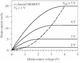
Typical currentvoltage characteristics of a longchannel MOSFET, where pinchoff is
the predominant saturation mechanism, are shown in the following figure.


However, with shorter MOSFET gate lengths, typically n the submicrometer range,
velocity saturation will occur in the channel near drain at lower VDS than that causing
pinchoff. This leads to more evenly spaced saturation characteristics than those shown in
this figure, more in agreement with those observed for modern devices. Also, phenomena
such as a finite channel conductance in saturation, a drain biasinduced shift in the
threshold voltage, and an increased subthreshold current are important consequences of
shorter gate lengths.


2.2.4 MOS Charge Control Model

2.2.4 MOS Charge Control Model

Well above threshold, the charge density of the mobile carriers in the inversion layer can
be calculated using the parallel plate charge control model of (2.28). This model gives an
adequate description for the strong inversion regime of the MOS capacitor, but fails for
applied voltages near and below threshold (i.e. in the weak inversion and depletion
regimes). Several expressions have been proposed for a unified charge control model
(UCCM) that covers all the regimes of operation, including the following:

where, a i c » c is approximately the insulator capacitance per unit area (with a small
correction for the finite vertical extent of the inversion channel), n0 = ns(V = VT) is the
density of minority carriers per unit area at threshold, and h is the socalled
subthreshold ideality factor, also known as the subthreshold swing parameter. The ideality factor
accounts for the subthreshold division of the applied voltage between the gate insulator
and the depletion layer, and the 1/h represents the fraction of this voltage that contributes
to the interface potential. A simplified analysis gives


This expression reproduces the correct limiting behaviour both in strong inversion and
the subthreshold regime, although it deviates slightly from (2.34) near threshold. The
various charge control expressions of the MOS capacitor are compared in the above
figure.


2.2.3 MOS Capacitance

2.2.3 MOS Capacitance

In a MOS capacitor, the metal contact and the neutral region in the doped semiconductor
substrate are separated by the insulator layer, the channel, and the depletion region.
Hence, the capacitance Cmos of the MOS structure can be represented as a series
connection of the insulator capacitance i i i C = S e d , where S is the area of the MOS
capacitor, and the capacitance of the active semiconductor layer Cs,

where Qs is the total charge per unit area in the semiconductor and y
s is the surface
potential. Using (2.9) to (2.12) for Qs and performing the differentiation , we obtain

here, s s Dp C = Se L 0 is the semiconductor capacitance at the flatband
condition (i.e., for
ys
=0) and LDp is the Debye length given by (2.11), equation (2.14) describes the
relationship between the surface and the applied bias.

The semiconductor capacitance can formally be represented as the sum of two
capacitancesa depletion layer capacitance, Cd and a free carrier capacitance Cfc. Cfc
together with a series resistance RGR describes the delay caused by thegeneration/
recombination mechanisms in the buildup and removal of inversion charge in
response to changes in the bias voltage. The depletion layer capacitance is given by

                                           d s d C = Se / d
is the depletion layer width. In strong inversion, a change in the applied voltage will
primarily affect the minority carrier charge at the interface, owing to the strong
dependence of this charge on the surface potential. This means that the depletion width
reaches a maximum value with no significant further increase in the depletion charge.
This maximum depletion width ddT can be determined from (2.23) by applying the
threshold condition, y s= 2jb. the corresponding minimum value of the depletion
capacitance is 
                                                CdT = S es / ddT.

As indicated, the variation in the minority carrier charge at the interface comes from the
processes of generation and recombination mechanisms, with the creation and removal of
electronhole pairs. Once an electronhole pair is generated, the majority carrier (a hole in
ptype material and an electron in ntype material) is swept from the space charge region
into the substrate by the electric field of this region. The minority carrier is swept in the
opposite direction toward semiconductorinsulator interface. The variation in the minority
carrier charge in the semiconductorinsulator interface therefore proceeds at a rate limited
by the time constants associated with the generation/recombination processes. This finite
rate represents a delay, which may be represented electrically in terms of an RC product
consisting of the capacitance Cfc and the resistance RGR, as reflected in the equivalent
circuit of the MOS structure shown in figure 2.7. The capacitance Cfc becomes important
in the inversion regime, especially in strong inversion where the mobile charge is
important. The resistance Rs in the equivalent circuit is the series resistance of the neutral
semiconductor layer and the contacts.


The calculated dependence of Cmos on the applied voltage for different frequencies is
shown in figure 2.8. For applied voltages well below threshold, the device is in accumulation
 and Cmos equals Ci. As the voltage approaches threshold, the semiconductor passes the 
flatband condition where Cmos has the value CFB, and then enters the depletion and weak
 inversion regimes where the depletion width increases and the capacitance value drops steadily
 until it reaches the minimum value at threshold given by (2.27). The calculated curves clearly
 demonstrate how the MOS capacitance in the strong inversion regime depends on the frequency, with a value of ¥ mos C at high frequencies to Ci at low frequencies.


We note that in a MOSFET, where the highly doped source and drain regions act as
reservoirs of minority carriers for the inversion layer, the time constant RGRCfc must be
19 substituted by a much smaller time constant corresponding to the time needed for
transporting carriers from these reservoirs in and out of the MOSFET gate area.Consequently,
 highfrequency strong inversion MOSFET gatechannel CV characteristics will resemble the
 zero frequency MOS characteristics.

2.2.2 Threshold Voltage

2.2.2 Threshold Voltage

The threshold voltage V=VT, corresponding to the onset of the strong inversion, is one of
the most important parameters characterizing metalinsulatorsemiconductor devices. As
discussed above, strong inversion occurs when the surface potential s y becomes equal to
2j b . For this surface potential, the charge of the free carriers induced at the insulator –
semiconductor interface is still small compared to the charge in the depletion layer, which
is given by


constant potential. Assuming that the inversion layer is grounded, VB biases the effective
junction between the inversion layer and the substrate, changing the amount of charge in
the depletion layer. In this case, the threshold voltage becomes
T FB b s a ( b B ) i V = V + 2j + 2e qN 2j - V c (2.18)


Note that the threshold voltage may also be affected by socalled fast surface states at the
semiconductoroxide interface and by fixed charges in the insulator layer. However, this
is not a significant concern with modern day fabrication technology.


As discussed above, the threshold voltage separates the subthreshold regime, where the
mobile carrier charge increases exponentially with increasing applied voltage, from the
abovethreshold regime, where the mobile carrier charge is linearly dependent on the
applied voltage.


2.2 The MOS Capacitor

To understand the MOSFET, it is convenient to analyze the MOS capacitor first, which
constitutes the important gatechannelsubstrate structure of the MOSFET. The MOS
capacitor is a two terminal semiconductor device of practical interest in its own right. As
indicated in figure 2.2, it consists of a metal contact separated from the semiconductor
substrate. Almost universally, the MOS structure utilizes doped silicon as the substrate
and its native oxide, SiO2, as the insulator. In the siliconsilicon dioxide system, the
density of surface states at the oxidesemiconductor interface is very low compared to the
typical channel carrier density in a MOSFET. Also, the insulating quality of the oxide is
quite good.


We assume that the insulator layer has infinite resistance, preventing any charge carrier
transport across the dielectric layer when a bias voltage is applied between the metal and
semiconductor. Instead, the applied voltage will induce charges and counter charges in
the metal and in the interface layer of the semiconductor, similar to what is expected in
the metal plates of a conventional parallel plate capacitor. However, in the MOS
capacitor we may use the applied voltage to control the type of interface charge we
induce in the semiconductor – majority carriers, minority carriers and depletion region.


Indeed, the ability to induce and modulate a conducting sheet of minority careers at the
semiconductor – oxide interface is the basis of the operation of the MOSFET.


2.2.1 Interface Charge
The induced interface charge in the MOS capacitor is closely linked to the shape of the
electron energy bands of the semiconductor near the interface. At zero applied voltage,
the bending of the energy bands are ideally determined by the difference in the work
functions of the metal and the semiconductor. This band bending changes with the
applied bias and the bands become flat when we apply the socalled flatband voltage
given by


where Fm and FS are the work functions of the metal and the semiconductor,
respectively, XS is the electron affinity for the semiconductor, Ec is the energy of the
conduction band edge and EF is the Fermi level at zero applied voltage. The various
energies involved are indicated in figure 2.3, where we show typical band diagrams of
    MOS capacitor at zero bias and with the voltage V=VFB applied to the metal contact
    relative to the semiconductoroxide interface.


    At stationary conditions, no net current flows in the direction perpendicular to the
    interface owing to the very high resistance of the insulator layer. Hence, the Fermi level
    will remain constant inside the semiconductor, independent of the biasing conditions.
    However, between the semiconductor and the metal contact, the Fermi level is shifted by
    EFM – EFS = qV (see Figure 2.3(b)). Hence, we have a quasiequilibrium
    situation in which the semiconductor can be treated as if in thermal equilibrium.


A MOS structure with a ptype semiconductor will enter the accumulation regime of
operation when the voltage applied between the metal and the semiconductor is more

negative than the flatband voltage (VFB < 0 in Figure 2.3). In the opposite case, when
V > VFB, the semiconductoroxide interface first becomes depleted of holes and we enter
the socalled depletion regime.


By increasing the applied voltage, the band bending becomes so large that the energy
difference between the Fermi level and the bottom of the conduction band at the
insulatorsemiconductor interface becomes smaller than that between the Fermi level and
the top of the valance band. This is the case indicated for V = 0V in Figure 2.3 (a).
Carrier statistics tells us that the electron concentration then will exceed the hole
concentration near the interface and we enter the inversion regime. At still larger applied
voltage, we finally arrive at a significant conducting sheet of inversion charge at the
interface.


The symbol y is used to signify the potential in the semiconductor measured relative to
the potential at a position x deep inside the semiconductor. To note that y becomes
positive when the bands bend down, as in the example of a ptype semiconductor shown
in Figure 2.4.


from equilibrium statistics, we find that the intrinsic Fermi level Ei in the bulk
corresponds to an energy separation qjb from the actual Fermi level EF of the doped
semiconductor,

          where Vth is the thermal voltage, Na is the shallow acceptor density in the ptype
semiconductor and ni is the intrinsic carrier density of silicon. According to the usual
definition, strong inversion is reached when the total band bending equals 2qjb,
corresponding to the surface potential y s = 2jb. Values of the surface potential such that
0 < y s < 2jb correspond to the depletion and the weak inversion regimes, y
s = 0 is the flatband condition, and y s < 0 corresponds to the accumulation mode.