2.3 Basic MOSFET Operation
In the MOSFET, an inversion layer at the semiconductoroxide interface acts as a
conducting channel. For example, in an nchannel MOSFET, the substrate is ptype
silicon and the inversion charge consists of electrons that form a conducting channel
between the n + ohmic source and the drain contacts. At DC conditions, the depletion
regions and the neutral substrate provide isolation between devices fabricated on the
same substrate. A schematic view of the nchannel MOSFET is shown in Figure 2.10.
As described above for the MOS capacitor, inversion charge can be induced in the
channel by applying a suitable gate voltage relative to other terminals. The onset of
strong inversion is defined in terms of a threshold voltage VT being applied to the gate
electrode relative to the other terminals. In order to assure that the induced inversion
channel extends all the way from source to drain, it is essential that the MOSFET gate
structure either overlaps slightly or aligns with the edges of these contacts (the latter is
achieved by a selfaligned process). Selfalignment is preferable since it minimizes the
parasitic gatesource and gatedrain capacitance.
When a drainsource bias VDS is applied to an nchannel MOSFET in the abovethreshold
conducting state, electrons move in the channel inversion layer from source to drain. A
change in the gatesource voltage VGS alters the electron sheet density in the channel,
modulating the channel conductance and the device current. For VGS > VT in an nchannel
device, an application of a positive VDS gives a steady voltage increase from
source to drain along the channel that causes a corresponding reduction in the local gatechannel
bias VGX (here X signifies a position x within the channel). This reduction is
greatest near drain where VGX equals the gatedrain bias VGD.
Somewhat simplistically, we may say that when VGD = VT, the channel reaches threshold
at the drain and the density of inversion charge vanishes at this point. This is the socalled
pinchoff condition, which leads to a saturation of the drain current Ids. The
corresponding drainsourcevoltage, VDS = VSAT, is called the saturation voltage. Since
VGD = VGS – VDS, we find that VSAT = VGS – VT.
When VDS > VSAT, the pinchedoff region near drain expands only slightly in the
direction of the source, leaving the remaining inversion channel intact. The point of
transition between the two regions, x = xp, is characterized by XS ( p ) SAT V x » V , where
( ) XS p V x is the channel voltage relative to source at the transition point. Hence, the drain
current in saturation remains approximately constant, given by the voltage drop VSAT
across the part of the channel that remains in inversion. The voltage VDS – VSAT across
the pinchedoff region creates a strong electric field, which efficiently transports the
electrons from the strongly inverted region to the drain.
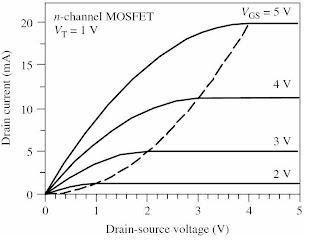
Typical currentvoltage characteristics of a longchannel MOSFET, where pinchoff is
the predominant saturation mechanism, are shown in the following figure.
However, with shorter MOSFET gate lengths, typically n the submicrometer range,
velocity saturation will occur in the channel near drain at lower VDS than that causing
pinchoff. This leads to more evenly spaced saturation characteristics than those shown in
this figure, more in agreement with those observed for modern devices. Also, phenomena
such as a finite channel conductance in saturation, a drain biasinduced shift in the
threshold voltage, and an increased subthreshold current are important consequences of
shorter gate lengths.


No comments:
Post a Comment